
The main function of a processor is to fetch, decode, and execute an instruction. As long as you trace how the fetching takes place, how the decoding takes place, and how the execution takes place you can understand the architecture and workflow of the Processor.
Here we also start with this, so a processor's first work is to fetch an instruction. To fetch the instruction the processor need to know the address of memory where the instruction stored and that address is given by a register called PC(Program Counter). PC always gives the address of the next instruction. as so as the instruction will fetch the PC get increment and pointing to the next address.
Fetching:-
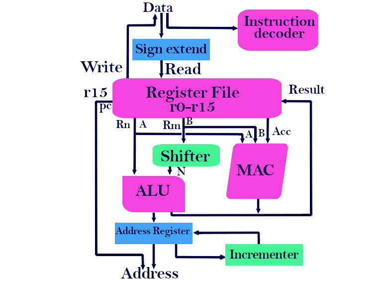
As I clearly mentioned in the introduction of ARM that ARM contains 37 registers, out of these 16 Registers(R0-R15) are available at any point in time. So the program starts with the register R15 which is called program counter. It takes the address from PC and sends it through 32 Bit address bus, through an address bus, we locate the address of the next instruction and fetch the instruction. And the instruction will come through the data bus. We know that instruction and data both come from the data bus. Because it follows Von Neumann architecture both instruction and data are stored in the same memory.
If an instruction is fetched from the memory then it goes to the instruction decoder. The instruction decoder decodes the instruction and generates control signals for its execution.
If data is fetched from the memory then it gets stored into the register file (R0-R15). All registers are 32-bits each. If the data fetched is lesser in size then it is sign-extended into 32-bits before being placed into the register file.
If data is fetched from the memory then it gets stored into the register file (R0-R15). All registers are 32-bits each. If the data fetched is lesser in size then it is sign-extended into 32-bits before being placed into the register file.
Decoding:-
Decoding is to analyzing the Upcode. Every instruction is stored in memory in the form of the binary value. ADD, SUB, MUL and all these instructions are not store as ADD, SUB, or MUL. Every instruction has a unique binary value. That is called Upcode. Decoding is to match the Upcode with its Instruction and send the control signal to all units as per the instruction. There are two types of control units in the world i.e hardwired and Micro-program. Hardwired is rigid but very fast. The microprogram is flexible but slow. As you know ARM is a performance-based processor that uses a hardwired control unit.
Execution:-
Now according to the instruction given by the control unit the execution will take place. The execution is done by ALU. ALU does the Arithmetic and logical operation with registers according to the control signal and results send back to the register.
The following things help the execution complete in exactly one cycle.
Sign Extend:-
When the Data comes from the data bus It could be 8-bit, 16-bit, or 32-bit not more than that because the data bus is of 32-bit. So if the data is of 8bit or 16bit then it needs to extend to 32-bit because it goes to a 32-bit register. So the extension operation is done by the sign extend function.
for ex:- if the data 00000101 then it extent to 00000000 00000101. Every time it's not blindly put zeros in remaining bits. That depends upon the sign bit of the data. let's say the data could be +5 or -5. The Binary of +5 is 0101 and of -5 is 1011(i.e the 2's complement of +5). To extend +5 it looks at the MSB i.e 0 so it put 12-bit as Zeros. And to extend -5 it looks at the MSB of the data 1011. Hence it has 1 in its MSB so it put the remaining 12-bit as 1(i.e 1111111111111011). It doesn't give any different value It gives exactly -5 because MSB of that value is 1 so it's a negative value first make 2's complement of that data then got the value with a negative sign. 2's complement of 1111111111111011 is 0000000000000101 which is 5 so that number was -5, that's how it is decided.
we can get an 8bit or 16bit data from the data bus and need to put the data in a 32-bit register for which we need the extended sign function in the diagram. i.e when we load the data from memory to register. But when we store the data from the register to memory we don't need that extend operator because the registers are of already 32-bit which is equal to the data bus size. So there is no need to extend.
ARM supports Triadic operation !!! What is that?
ex:- ADD R0 R1 R2
What do you think that is the addition of R0+R1+R2 ..? NO.
That means R0=R1+R2. Add R1 with R2 and store the result in R0. We can't add 3 registers at a time, there is a reason behind it. i.e carry bit. As we know to store carry of some operation we have only one bit that can store either 0 or 1. So If we add two biggest one-digit numbers let's say 9+9 gives the result 18. Here the carry is 1. But if we add 3 number 9+9+9 results 27 which carry is 2 but we have only one bit to store the carry. That's why we can't add 3 registers at a time.
Then what is the use of triadic operation..! Of course, there are. It gives the freedom to add two registers and put the result in a third register.
Look when we write ADD R0, R1; it adds R0 with R1 and stores the result in R0. As well as we get the result the register R0 loss it's original value. But by triadic (ADD R0, R1, R2) the result of R1 and R2 is stored in R0, so here no register loses its values we can do any further operation using that register R1 or R2. If we want to overwrite the value we can write as ADD R0, R0, R1, and ADD R0, R0, R0 which means add R0 with R1, and put the result in R0. Similarly, add R0 with R0, and put the result also in R0.
Shifter:-
Some people irritating by seeing the shifter or barrel shifter in the picture or even in the official pic of the ARM processor. Don't confuse between shift and a barrel shifter. all the shifters are barrel shifter. and there work is to shift all the bits at a time. This shifter comes to use when the instruction addressing mode is base on the scaled index addressing mode. That scale means to shift left or right as per the instruction. It does two things together Shift and addition. It gives one operand directly and the other operand shifted and provided. So instead of using a separate instruction for shifting Here the single instruction use to shift and provide the operand to operation. we use the base with scale addressing mode.
MAC:-
Again there is a dedicated circuit called MAC i.e multiply and accumulate.
It is used when the instruction MLA is provided. It is used for numbers of multiplication. In multiplication, we multiply each digit of multiplier with multiplicand and add all the results and get the final result. If the multiplier is of 2 digits then we get 2 partial results similarly when we multiply two 64bit the partial result also we get 64. The processor doesn't have the memory to store all the partial results and add them later. That's why the accumulator in this circuit accumulates the partial results and gives the final result.
So take one register to initialize it with zero. Then every time you multiply results will be added with that register. These called multiply and accumulate. MLA R0 R1 R2
Address Register:-
In base index addressing mode the address is given by the sum of two registers. So here to fetch data the address comes from two registers and the sum is calculated by ALU. And then the ALU put the address to the address bus to fetch the data. But before it put into the address bus it saves the address into a register called Address register. Because When we increment the register we can get the subsequent location to do the operation no need of ALU again to calculate the sum.
For example:- The two register gives the addresses 3000(as a base) and 1000(as index). then the sum is calculated by ALU and put the value 4000 in address bus through address register. So if the instruction needs to access the series of locations from there. ( For 32 Bit operation subsequent addresses 4004,4008,4012 and so on..) then we don't need to disturb ALU to calculate the some each time. We just need to increment the address register.


